原文地址:http://mechanical-sympathy.blogspot.com/2013/02/cpu-cache-flushing-fallacy.html (因有墙移动到墙内)
Even from highly experienced technologists I often hear talk about how certain operations cause a CPU cache to “flush”. This seems to be illustrating a very common fallacy about how CPU caches work, and how the cache sub-system interacts with the execution cores. In this article I will attempt to explain the function CPU caches fulfil, and how the cores, which execute our programs of instructions, interact with them. For a concrete example I will dive into one of the latest Intel x86 server CPUs. Other CPUs use similar techniques to achieve the same ends.
Most modern systems that execute our programs are shared-memory multi-processor systems in design. A shared-memory system has a single memory resource that is accessed by 2 or more independent CPU cores. Latency to main memory is highly variable from 10s to 100s of nanoseconds. Within 100ns it is possible for a 3.0GHz CPU to process up to 1200 instructions. Each Sandy Bridge core is capable of retiring up to 4 instructions-per-cycle (IPC) in parallel. CPUs employ cache sub-systems to hide this latency and allow them to exercise their huge capacity to process instructions. Some of these caches are small, very fast, and local to each core; others are slower, larger, and shared across cores. Together with registers and main-memory, these caches make up our non-persistent memory hierarchy.
Next time you are developing an important algorithm, try pondering that a cache-miss is a lost opportunity to have executed ~500 CPU instructions! This is for a single-socket system, on a multi-socket system you can effectively double the lost opportunity as memory requests cross socket interconnects.
Memory Hierarchy
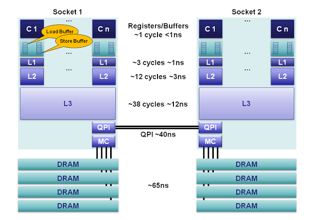 |
| Figure 1. |
For the circa 2012 Sandy Bridge E class servers our memory hierarchy can be decomposed as follows:
- Registers: Within each core are separate register files containing 160 entries for integers and 144 floating point numbers. These registers are accessible within a single cycle and constitute the fastest memory available to our execution cores. Compilers will allocate our local variables and function arguments to these registers. Whenhyperthreading is enabled these registers are shared between the co-located hyperthreads.
- Memory Ordering Buffers (MOB): The MOB is comprised of a 64-entry load and 36-entry store buffer. These buffers are used to track in-flight operations while waiting on the cache sub-system. The store buffer is a fully associative queue that can be searched for existing store operations, which have been queued when waiting on the L1 cache. These buffers enable our fast processors to run asynchronously while data is transferred to and from the cache sub-system. When the processor issues asynchronous reads and writes then the results can come back out-of-order. The MOB is used to disambiguate the load and store ordering for compliance to the published memory model.
- Level 1 Cache: The L1 is a core-local cache split into separate 32K data and 32K instruction caches. Access time is 3 cycles and can be hidden as instructions are pipelined by the core for data already in the L1 cache.
- Level 2 Cache: The L2 cache is a core-local cache designed to buffer access between the L1 and the shared L3 cache. The L2 cache is 256K in size and acts as an effective queue of memory accesses between the L1 and L3. L2 contains both data and instructions. L2 access latency is 12 cycles.
- Level 3 Cache: The L3 cache is shared across all cores within a socket. The L3 is split into 2MB segments each connected to a ring-bus network on the socket. Each core is also connected to this ring-bus. Addresses are hashed to segments for greater throughput. Latency can be up to 38 cycles depending on cache size. Cache size can be up to 20MB depending on the number of segments, with each additional hop around the ring taking an additional cycle. The L3 cache is inclusive of all data in the L1 and L2 for each core on the same socket. This inclusiveness, at the cost of space, allows the L3 cache to intercept requests thus removing the burden from private core-local L1 & L2 caches.
- Main Memory: DRAM channels are connected to each socket with an average latency of ~65ns for socket local access on a full cache-miss. This is however extremely variable, being much less for subsequent accesses to columns in the same row buffer, through to significantly more when queuing effects and memory refresh cycles conflict. 4 memory channels are aggregated together on each socket for throughput, and to hide latency via pipelining on the independent memory channels.
- NUMA: In a multi-socket server we have non-uniform memory access. It is non-uniform because the required memory maybe on a remote socket having an additional 40ns hop across the QPI bus. Sandy Bridge is a major step forward for 2-socket systems over Westmere and Nehalem. With Sandy Bridge the QPI limit has been raised from 6.4GT/s to 8.0GT/s, and two lanes can be aggregated thus eliminating the bottleneck of the previous systems. For Nehalem and Westmere the QPI link is only capable of ~40% the bandwidth that could be delivered by the memory controller for an individual socket. This limitation made accessing remote memory a choke point. In addition, the QPI link can now forward pre-fetch requests which previous generations could not.
Associativity Levels
Caches are effectively hardware based hash tables. The hash function is usually a simple masking of some low-order bits for cache indexing. Hash tables need some means to handle a collision for the same slot. The associativity level is the number of slots, also known as ways or sets, which can be used to hold a hashed version of an address. Having more levels of associativity is a trade off between storing more data vs. power requirements and time to search each of the ways.
For Sandy Bridge the L1D and L2 are 8-way associative, the L3 is 12-way associative.
Cache Coherence
With some caches being local to cores, we need a means of keeping them coherent so all cores can have a consistent view of memory. The cache sub-system is considered the “source of truth” for mainstream systems. If memory is fetched from the cache it is never stale; the cache is the master copy when data exists in both the cache and main-memory. This style of memory management is known as write-back whereby data in the cache is only written back to main-memory when the cache-line is evicted because a new line is taking its place. An x86 cache works on blocks of data that are 64-bytes in size, known as a cache-line. Other processors can use a different size for the cache-line. A larger cache-line size reduces effective latency at the expense of increased bandwidth requirements.
To keep the caches coherent the cache controller tracks the state of each cache-line as being in one of a finite number of states. The protocol Intel employs for this is MESIF, AMD employs a variant know as MOESI. Under the MESIF protocol each cache-line can be in 1 of the 5 following states:
- Modified: Indicates the cache-line is dirty and must be written back to memory at a later stage. When written back to main-memory the state transitions to Exclusive.
- Exclusive: Indicates the cache-line is held exclusively and that it matches main-memory. When written to, the state then transitions to Modified. To achieve this state a Request-For-Ownership (RFO) message is sent which involves a read plus an invalidate broadcast to all other copies.
- Shared: Indicates a clean copy of a cache-line that matches main-memory.
- Invalid: Indicates an unused cache-line.
- Forward: Indicates a specialised version of the shared state i.e. this is the designated cache which should respond to other caches in a NUMA system.
To transition from one state to another, a series of messages are sent between the caches to effect state changes. Previous to Nehalem for Intel, and Opteron for AMD, this cache coherence traffic between sockets had to share the memory bus which greatly limited scalability. These days the memory controller traffic is on a separate bus. The Intel QPI, and AMD HyperTransport, buses are used for cache coherence between sockets.
The cache controller exists as a module within each L3 cache segment that is connected to the on-socket ring-bus network. Each core, L3 cache segment, QPI controller, memory controller, and integrated graphics sub-system are connected to this ring-bus. The ring is made up of 4 independent lanes for: request, snoop, acknowledge, and 32-bytesdata per cycle. The L3 cache is inclusive in that any cache-line held in the L1 or L2 caches is also held in the L3. This provides for rapid identification of the core containing a modified line when snooping for changes. The cache controller for the L3 segment keeps track of which core could have a modified version of a cache-line it owns.
If a core wants to read some memory, and it does not have it in a Shared, Exclusive, or Modified state; then it must make a read on the ring bus. It will then either be read from main-memory if not in the cache sub-systems, or read from L3 if clean, or snooped from another core if Modified. In any case the read will never return a stale copy from the cache sub-system, it is guaranteed to be coherent.
Concurrent Programming
If our caches are always coherent then why do we worry about visibility when writing concurrent programs? This is because within our cores, in their quest for ever greater performance, data modifications can appear out-of-order to other threads. There are 2 major reasons for this.
Firstly, our compilers can generate programs that store variables in registers for relatively long periods of time for performance reasons, e.g. variables used repeatedly within a loop. If we need these variables to be visible across cores then the updates must not be register allocated. This is achieved in C by qualifying a variable as “volatile”. Beware that C/C++ volatile is inadequate for telling the compiler not to reorder other instructions. For this you need memory fences/barriers.
The second major issue with ordering we have to be aware of is a thread could write a variable and then, if it reads it shortly after, could see the value in its store buffer which may be older than the latest value in the cache sub-system. This is never an issue for algorithms following the Single Writer Principle but is an issue for the likes of the Dekker andPeterson lock algorithms. To overcome this issue, and ensure the latest value is observed, the thread must not load the value in the local store buffer. This can be achieved by issuing a fence instruction which prevents the subsequent load getting ahead of a store from another thread. The write of a volatile variable in Java, in addition to never being register allocated, is accompanied by a full fence instruction. This fence instruction on x86 has a significant performance impact by preventing progress on the issuing thread until the store buffer is drained. Fences on other processors can have more efficient implementations that simply put a marker in the store buffer for the search boundary, e.g. the Azul Vega does this.
If you want to ensure memory ordering across Java threads when following the Single Writer Principle, and avoid the store fence, it is possible by using the j.u.c.Atomic(Int|Long|Reference).lazySet() method, as opposed to setting a volatile variable.
The Fallacy
Returning to the fallacy of “flushing the cache” as part of a concurrent algorithm. I think we can safely say that we never “flush” the CPU cache within our user space programs. I believe the source of this fallacy is the need to flush, mark or drain to a point, the store buffer for some classes of concurrent algorithms so the latest value can be observed on a subsequent load operation. For this we require a memory ordering fence and not a cache flush.
Another possible source of this fallacy is that L1 caches, or the TLB, may need to be flushed based on address indexing policy on a context switch. ARM, previous to ARMv6, did not use address space tags on TLB entries thus requiring the whole L1 cache to be flushed on a context switch. Many processors require the L1 instruction cache to be flushed for similar reasons, in many cases this is simply because instruction caches are not required to be kept coherent. The bottom line is, context switching is expensive and a bit off topic, so in addition to the cache pollution of the L2, a context switch can also cause the TLB and/or L1 caches to require a flush. Intel x86 processors require only a TLB flush on context switch.